- 您现在的位置:买卖IC网 > Sheet目录1992 > CY28442ZXC-2 (Silicon Laboratories Inc)IC CLOCK ALVISO PENTM 56TSSOP
CY28442-2
....................... Document #: 38-07691 Rev. *B Page 7 of 19
0
CPU[T/C]0
CPU[T/C]0 PWRDWN Drive Mode
0 = Driven when PD asserted,1 = Tri-state when PD asserted
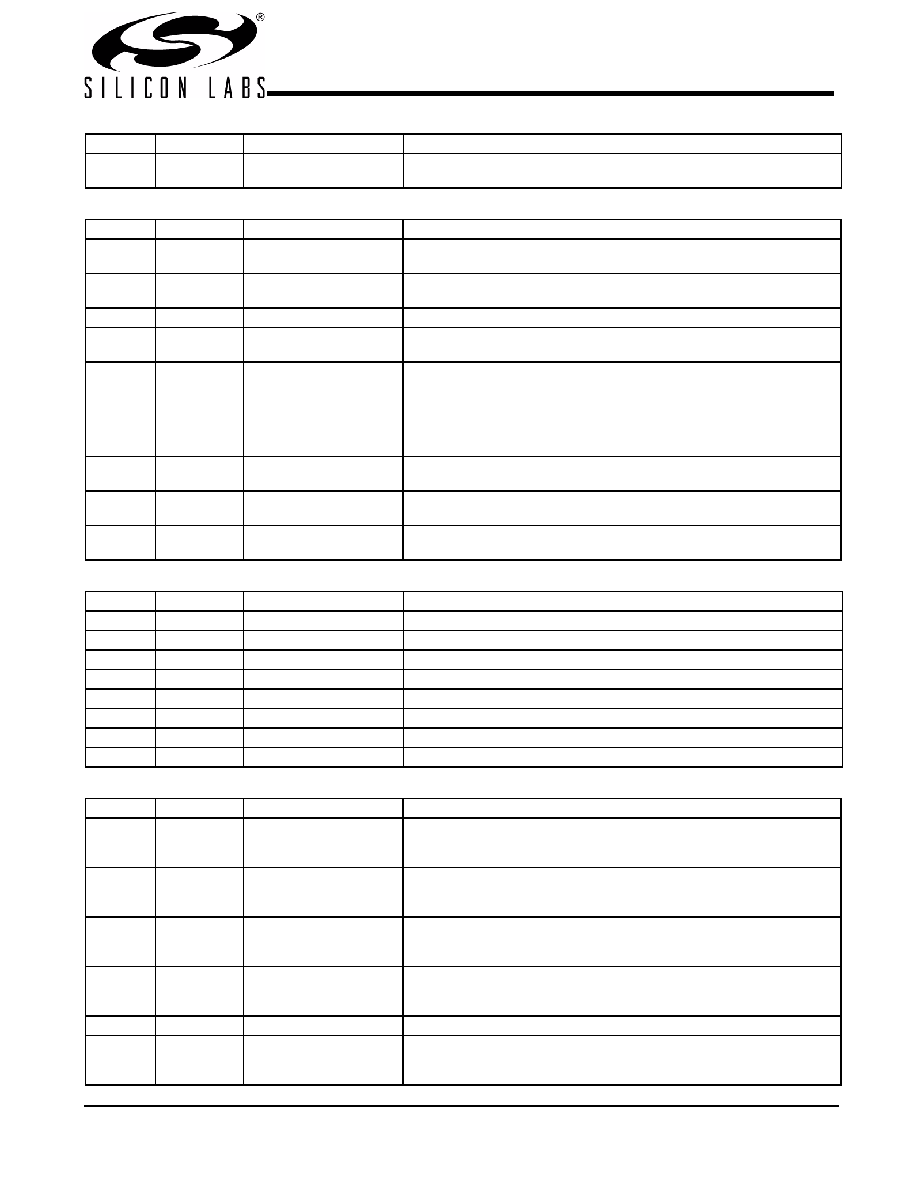
Byte 6: Control Register 6
Bit
@Pup
Name
Description
7
0
TEST_SEL
REF/N or Tri-state Select
0 = Tri-state, 1 = REF/N Clock
6
0
TEST_MODE
Test Clock Mode Entry Control
0 = Normal operation, 1 = REF/N or Tri-state mode,
5
0
RESERVED
4
1
REF
REF Output Drive Strength
0 = Low, 1 = High
3
1
PCI, PCIF and SRC clock
outputs except those set
to free running
SW PCI_STP Function
0=SW PCI_STP assert, 1= SW PCI_STP deassert
When this bit is set to 0, all STOPPABLE PCI, PCIF and SRC outputs will
be stopped in a synchronous manner with no short pulses.
When this bit is set to 1, all STOPPED PCI, PCIF and SRC outputs will
resume in a synchronous manner with no short pulses.
2
HW
FS_C
FS_C Reflects the value of the FS_C pin sampled on power-up
0 = FS_C was low during VTT_PWRGD# assertion
1
HW
FS_B
FS_B Reflects the value of the FS_B pin sampled on power-up
0 = FS_B was low during VTT_PWRGD# assertion
0
HW
FS_A
FS_A Reflects the value of the FS_A pin sampled on power-up
0 = FS_A was low during VTT_PWRGD# assertion
Byte 7: Vendor ID
Bit
@Pup
Name
Description
7
0
Revision Code Bit 3
6
0
Revision Code Bit 2
5
0
Revision Code Bit 1
4
0
Revision Code Bit 0
3
1
Vendor ID Bit 3
2
0
Vendor ID Bit 2
1
0
Vendor ID Bit 1
0
Vendor ID Bit 0
Byte 8: Control Register 8
Bit
@Pup
Name
Description
7
0
CLKREQ#B
SRC[T/C]7CLKREQ#B control
1 = SRC[T/C]7 stoppable by CLKREQ#B pin
0 = SRC[T/C]7 not controlled by CLKREQ#B pin
6
1
CLKREQ#B
SRC[T/C]5 CLKREQ#B control
1 = SRC[T/C]5 stoppable by CLKREQ#B pin
0 = SRC[T/C]5 not controlled by CLKREQ#B pin
5
0
CLKREQ#B
SRC[T/C]3 CLKREQ#B control
1 = SRC[T/C]3 stoppable by CLKREQ#B pin
0 = SRC[T/C]3 not controlled by CLKREQ#B pin
4
0
CLKREQ#B
SRC[T/C]1 CLKREQ#B control
1 = SRC[T/C]1 stoppable by CLKREQ#B pin
0 = SRC[T/C]1 not controlled by CLKREQ#B pin
3
0
RESERVED
2
1
CLKREQ#A
SRC[T/C]4 CLKREQ#A control
1 = SRC[T/C]4 stoppable by CLKREQ#A pin
0 = SRC[T/C]4 not controlled by CLKREQ#A pin
Byte 5: Control Register 5 (continued)
Bit
@Pup
Name
Description
发布紧急采购,3分钟左右您将得到回复。
相关PDF资料
CY28445LFXC-5
IC CLOCK CALISTOGA CK410M 68QFN
CY28446LFXC
IC CLOCK CALISTOGA CK410M 64QFN
CY28447LFXC
IC CLOCK CALISTOGA CK410M 72QFN
CY28547LFXCT
IC CLOCK CK505/410M INTEL 72QFN
CY28548ZXC
IC CLK CK505 960M/965M 64TSSOP
CY28551LFXC-3T
IC CLOCK INTEL/AMD SIS VIA 56QFN
CY28551LFXC
IC CLOCK INTEL/AMD SIS VIA 64QFN
CY2SSTV855ZXI
IC CLOCK DIFFDRV PLL DDR 28TSSOP
相关代理商/技术参数
CY28442ZXC-2T
功能描述:时钟发生器及支持产品 Calistoga RoHS:否 制造商:Silicon Labs 类型:Clock Generators 最大输入频率:14.318 MHz 最大输出频率:166 MHz 输出端数量:16 占空比 - 最大:55 % 工作电源电压:3.3 V 工作电源电流:1 mA 最大工作温度:+ 85 C 安装风格:SMD/SMT 封装 / 箱体:QFN-56
CY28442ZXCT
功能描述:IC CLOCK GEN ALVISO 56-TSSOP RoHS:是 类别:集成电路 (IC) >> 时钟/计时 - 时钟发生器,PLL,频率合成器 系列:- 产品变化通告:Product Discontinuation 04/May/2011 标准包装:96 系列:- 类型:时钟倍频器,零延迟缓冲器 PLL:带旁路 输入:LVTTL 输出:LVTTL 电路数:1 比率 - 输入:输出:1:8 差分 - 输入:输出:无/无 频率 - 最大:133.3MHz 除法器/乘法器:是/无 电源电压:3 V ~ 3.6 V 工作温度:0°C ~ 70°C 安装类型:表面贴装 封装/外壳:16-TSSOP(0.173",4.40mm 宽) 供应商设备封装:16-TSSOP 包装:管件 其它名称:23S08-5HPGG
CY28443
制造商:CYPRESS 制造商全称:Cypress Semiconductor 功能描述:Clock Generator for Intel㈢ Calistoga Chipset
CY28443-2
制造商:CYPRESS 制造商全称:Cypress Semiconductor 功能描述:Clock Generator for Intel㈢ Calistoga Chipset
CY28443-3
制造商:SPECTRALINEAR 制造商全称:SPECTRALINEAR 功能描述:Clock Generator for Intel㈢ Calistoga Chipset
CY28443OXC
制造商:CYPRESS 制造商全称:Cypress Semiconductor 功能描述:Clock Generator for Intel㈢ Calistoga Chipset
CY28443OXC-2
制造商:CYPRESS 制造商全称:Cypress Semiconductor 功能描述:Clock Generator for Intel㈢ Calistoga Chipset
CY28443OXC-2T
制造商:CYPRESS 制造商全称:Cypress Semiconductor 功能描述:Clock Generator for Intel㈢ Calistoga Chipset